Related information
 A-Probe Guide
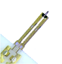
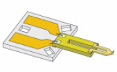
What is A-Probe?
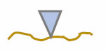
How it works?
What can be done?
 Magnetic Force (preliminary test)
 Use in SEM
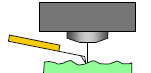
 Quasi contact mode
Akiyama-Probe Gallery
| EMPA Switzerland Dr. Vinzenz Friedli, “Focused electron- and ion-beam induced processes : in situ monitoring, analysis and modeling,” disseration EPFL, no 4036 (2008). |
|
|
Akiyama-Probe in SEM
|

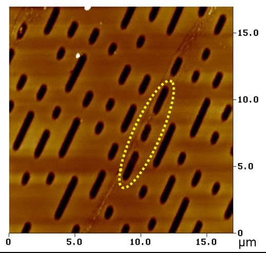
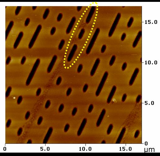
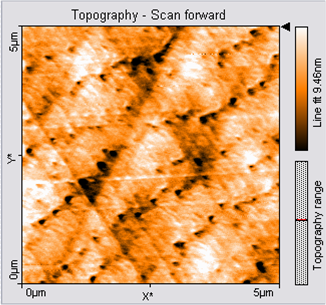
| Institute of Microtechnology, University of Neuchâtel, Switzerland on Veeco Nanoscope III, with Nanosurf easyPLL |
|
|
Akiyama-Probe vs. Optical lever
|
|
 |
 |
| Akiyama-Probe | Std. 40 N/m Si lever, Tapping mode |
| Research Institute of Biomolecule Metrology Co., Ltd., Japan SXM Standard |
|
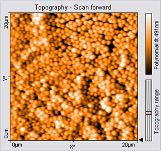
| Topographic images taken under ambient conditions in intermittent contact mode using Akiyama-Probe with : SXM Standard (Research Institute of Biomolecule Metrology Co., Ltd., Japan) |
|
 |
| Institute of Microtechnology, University of Neuchâtel, Switzerland on Veeco Nanoscope III, with Nanosurf easyPLL | |
| Samples from Nanosurf AG. | |
 |
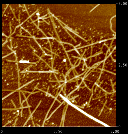 |
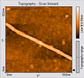
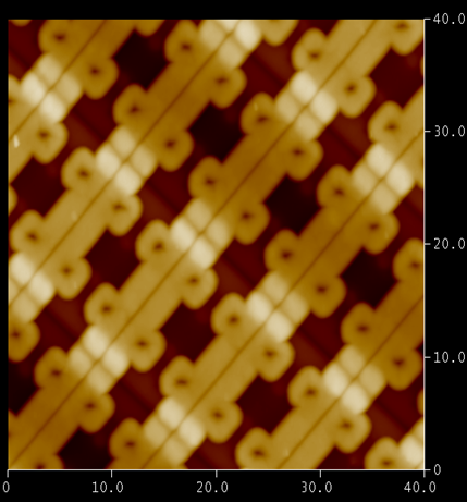
| IC chip (40 µm x 40 µm) | Carbon nanotube (5 µm x 5 µm) |
 |
 |
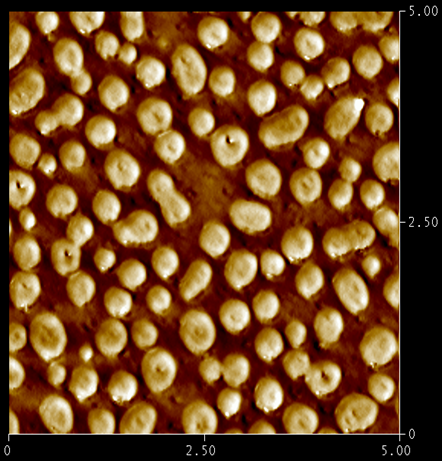
| PS/PMMA film (5 µm x 5 µm) | Glass beads (4 µm x 4 µm) |
NANOSENSORS™ is a trademark of NanoWorld AG - Copyright by NanoWorld AG